• Hello! As you may have gathered from the general gist of the website, I’ve decided to start a good old-fashioned blog. The main use of this blog will be to document my thoughts on various projects, not just for other people to read, but so I can keep track of it myself as projects become increasingly complex. My primary ongoing project is currently a polyphonic analogue synthesiser and you join me about bang in the middle of the development. I have completed the rough design of the synth but there is still much to develop and fine tune, and always more to learn.

    As I progress into assembling and coding the microprocessor for the synth, I’d like to have a record of the analogue electronics for myself to reference, as my schematics can’t fit all the theory into the notes. I’m going to aim the content of this to people who know the foundations of synths, (you know what an oscillator, a filter and an envelope is), but don’t necessarily know all too much about the internal circuitry of audio equipment. A basic understanding of electronics (ie what a capacitor is) is presumed for brevity’s sake. I’d like to keep the tone light but we may get into some maths at some point down the line. Maybe you’re thinking about starting your own project and want some guidance or advice? I’m by no means an electrical engineer but perhaps you can avoid some of the same mistakes I’ve made on this journey and use this page as a resource to get your head around the basics.

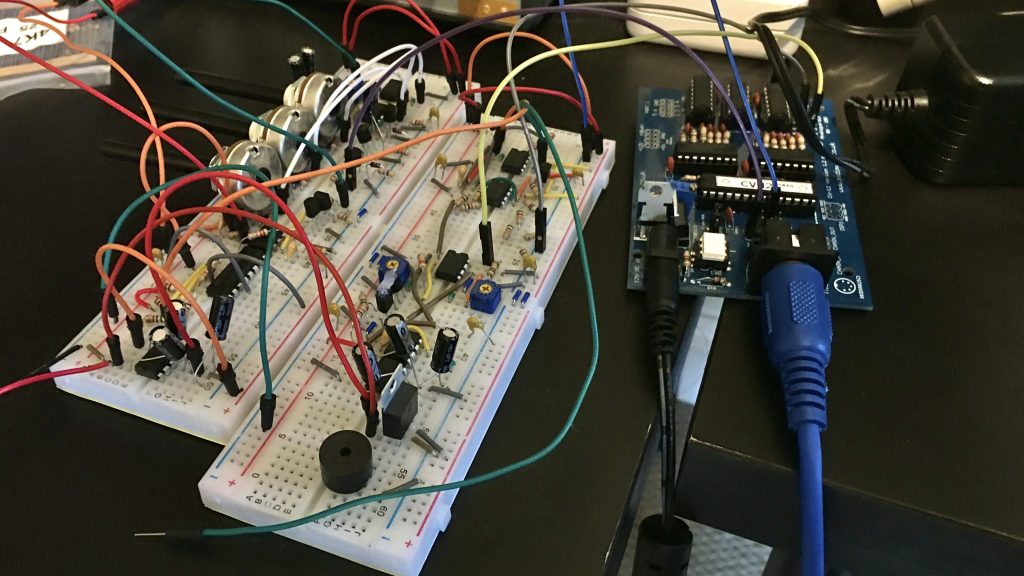
    An early monophonic experiment from years past

    So what is this synth?

    I set out with a fairly simple goal: to build myself a polyphonic synth. I’ve built monophonic synths before at school and college, but it had mostly been on breadboards and I didn’t entirely know what I was doing. This was to be a leap forward. It soon became apparent to me that polyphonic synths are preposterously complex machines with a lot of electronics and generally clever shit going on. As I continued to develop the synth, I realised that if I was going to be bothered to put enough effort in to make the polyphony work, I might as well make the synth as powerful and as feature packed as I could. The specs have changed vastly from the original idea over a year ago and are still being changed slightly but here’s a nerdy spec list in full:

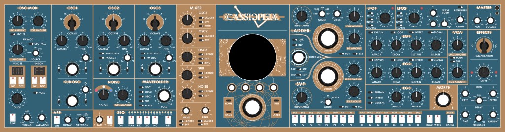
    • 16 voices, each with:
      • 3x oscillators (saw/pulse/tri/sine)
      • 1x sub osc derived from osc1 (saw/square/tri/sine)
      • Pink/white/blue noise
      • Assignable Hard sync
      • Assignable FM
      • Assignable Ring mod
      • Assignable Wavefolder
      • 2x ext input
      • 2x analogue ADSR EG (Pitch/filter, filter/amp)
      • 1x analogue AR EG for noise contouring
      • 2x analogue LFO (multi-wave, and a tri only for vibrato)
      • 2x VCF (ladder and state variable)
      • 1x VCA
      • Each source to be routable to each filter, the Wavefolder, or direct to the VCA
    • Global features:
      • 2x assignable utility Digital DAHDSR
      • 2x assignable utility Digital LFO
      • Digital Modulation matrix
      • Voice autotune
      • Full recall/presets
      • Assignable voice allocation
      • Split 8/8 voice patches
      • Analogue Chorus/drive/delay global effects
    • 61 key keyboard with polyphonic aftertouch
    • Ribbon controller
    • XY pad
    • Hardwood case and front panel!

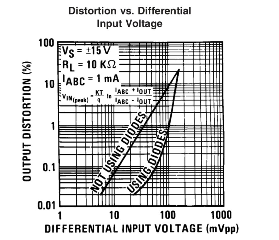
    This list is big and expensive. Another obstacle I set myself was not to use any “do it for you” integrated circuits. That includes the AS33xx chips etc found in the prophet 5 and many other poly synths that would simply generate the waveforms or produce an envelope for me. This has to be proper diy otherwise what’s the point of trying to learn how an oscillator works if it’s built into a package for you? I allowed myself simple operational amplifiers, transistors, and transconductance operational amplifiers as well as the shift registers and multiplexers required for the digital side. It seems impractical but actually the voice card is designed and soon to be prototyped. That being said I make a lot of mistakes, and I am far from an electronics guru. I am learning from this process and the main point of this project is as a “thrown in the deep end” learning experience. I may also add a lower manual of 88 keys with monophonic aftertouch but I’ll cross that bridge when I get to it…

    Ok then, what’s the overall architechture?

    One of the hardest problems with a poly synth (other than tuning oh my god) is that every parameter must be voltage controlled. If you have an 8 voice synth you can’t really have a variable resistor in circuit to tweak a parameter such as the cutoff for a filter as you’d have to have an 8 gang potentiometer which don’t really exist or are prohibitively expensive and impractical. Instead a single voltage can be generated and sent to each control voltage (CV) input on each of the voice cards to somehow drive a change in the behaviour of the circuit. This is achieved in a multitude of ways in practice but rarely is it straightforward and it often adds a variety of additional parts.

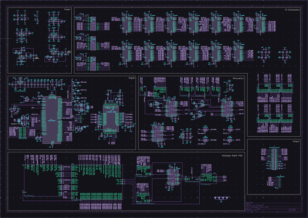
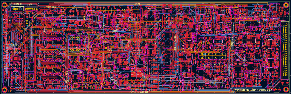
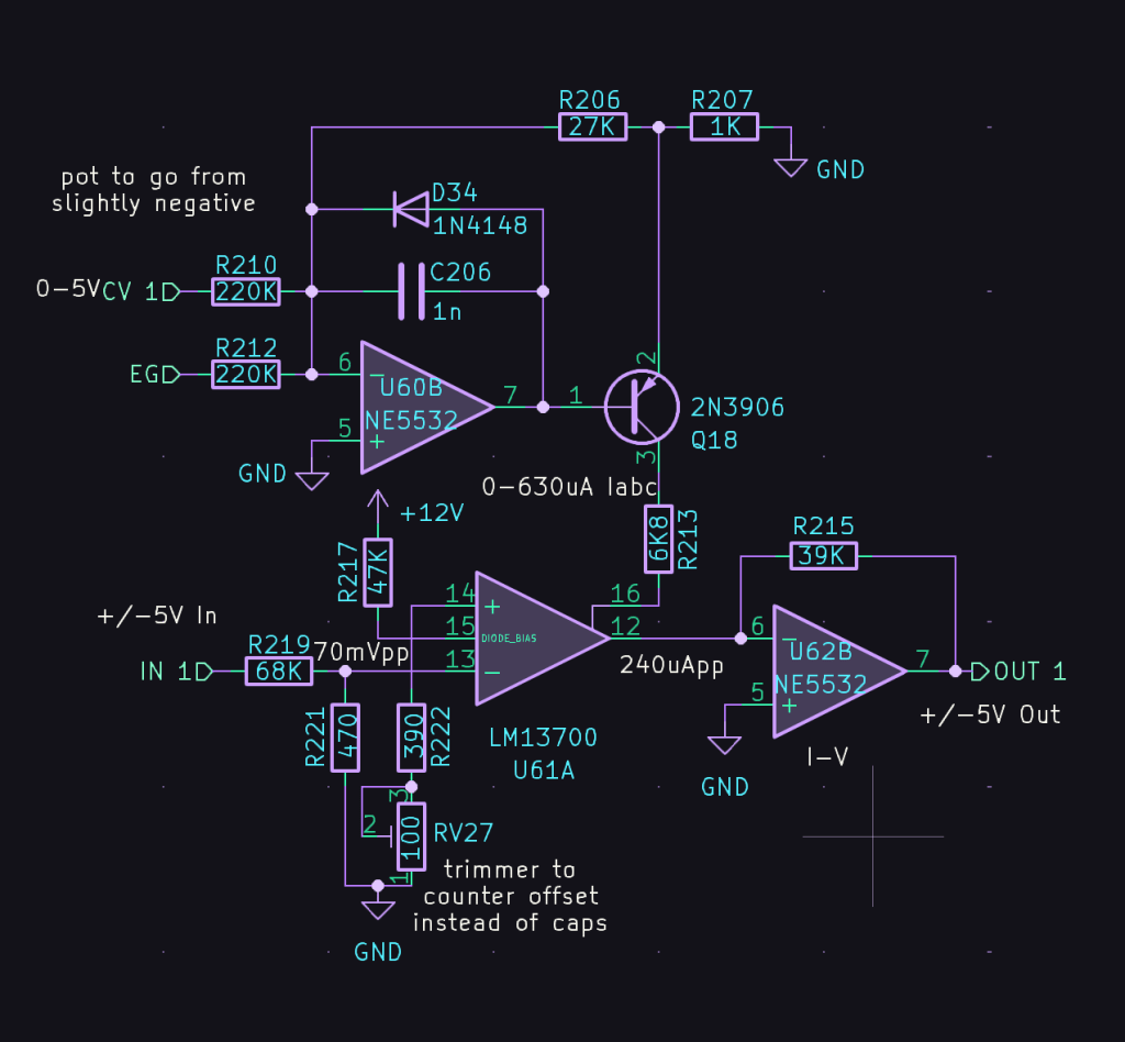
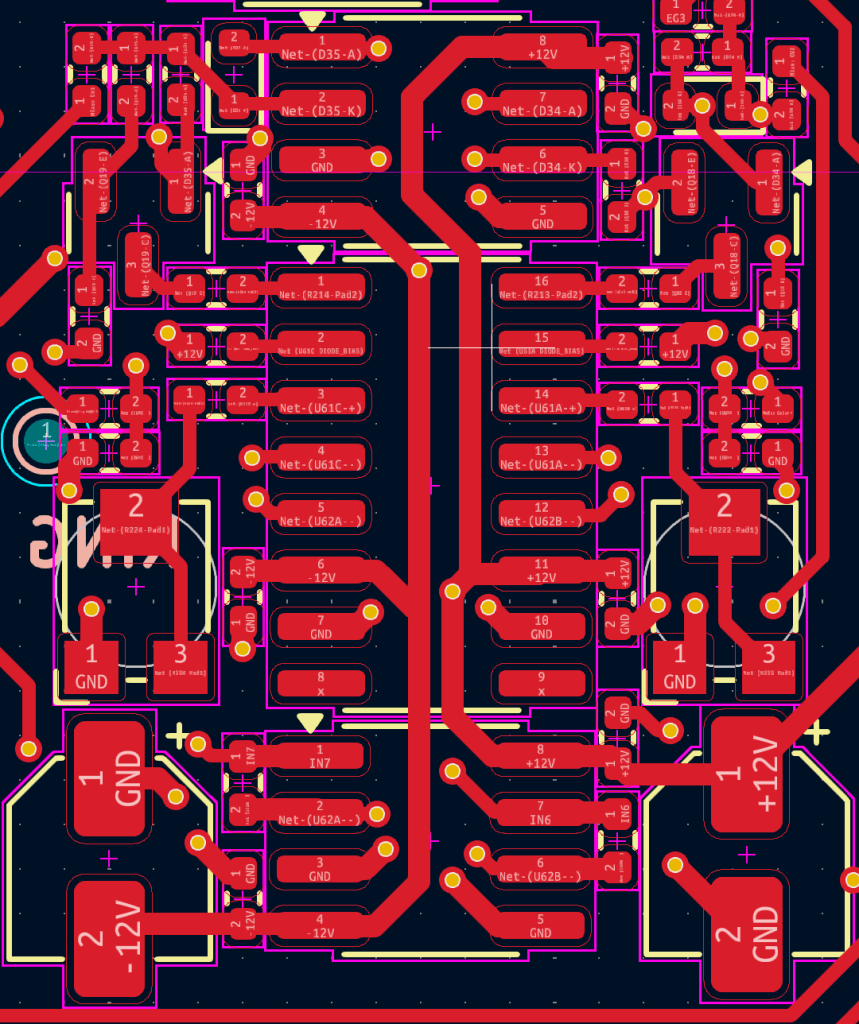
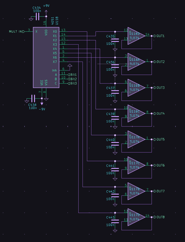
    The root page of the voice card schematic. There are many, many sub circuits and additional pages not pictured here.

    For my synth I opted to have the front panel with the knobs generate a voltage which is sampled by an analogue to digital convertor (ADC) in a master microprocessor. Once digitised, these voltages are sent digitally to each voice card which has its own local microprocessor. The local MCU then converts back to +/-5V analogue and distributes all the control voltages to various points in the circuit to control parameters. Each voice card audio output is summed on a final board which has the chorus, delay and distortion effects and outputted at line level. Obviously it’s much much more complex once you drill into the nitty gritty and I’ll make a post on each section as I go, but that’s the general idea! This architecture is used in a more or less similar fashion on all polyphonic synths including the Prophet 5, Jupiter 8, Moog One etc etc. 

    Where am I at currently?

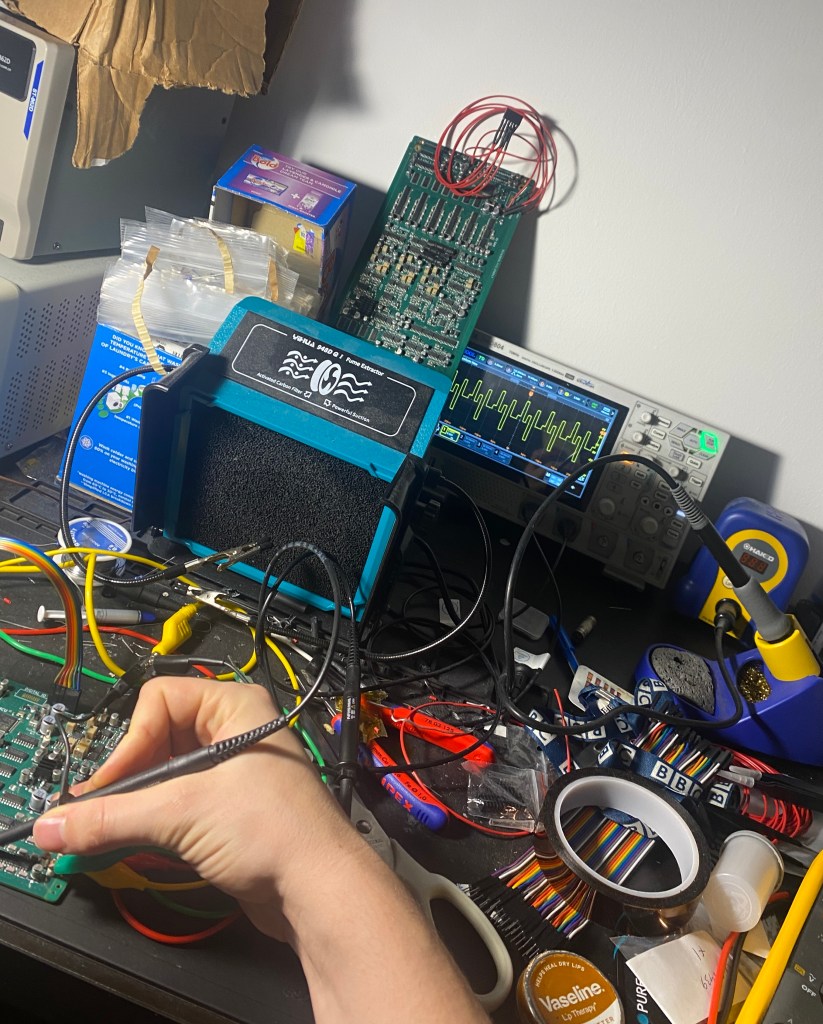
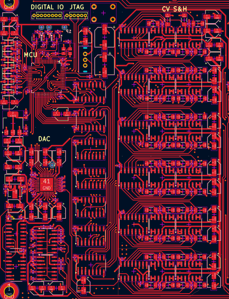
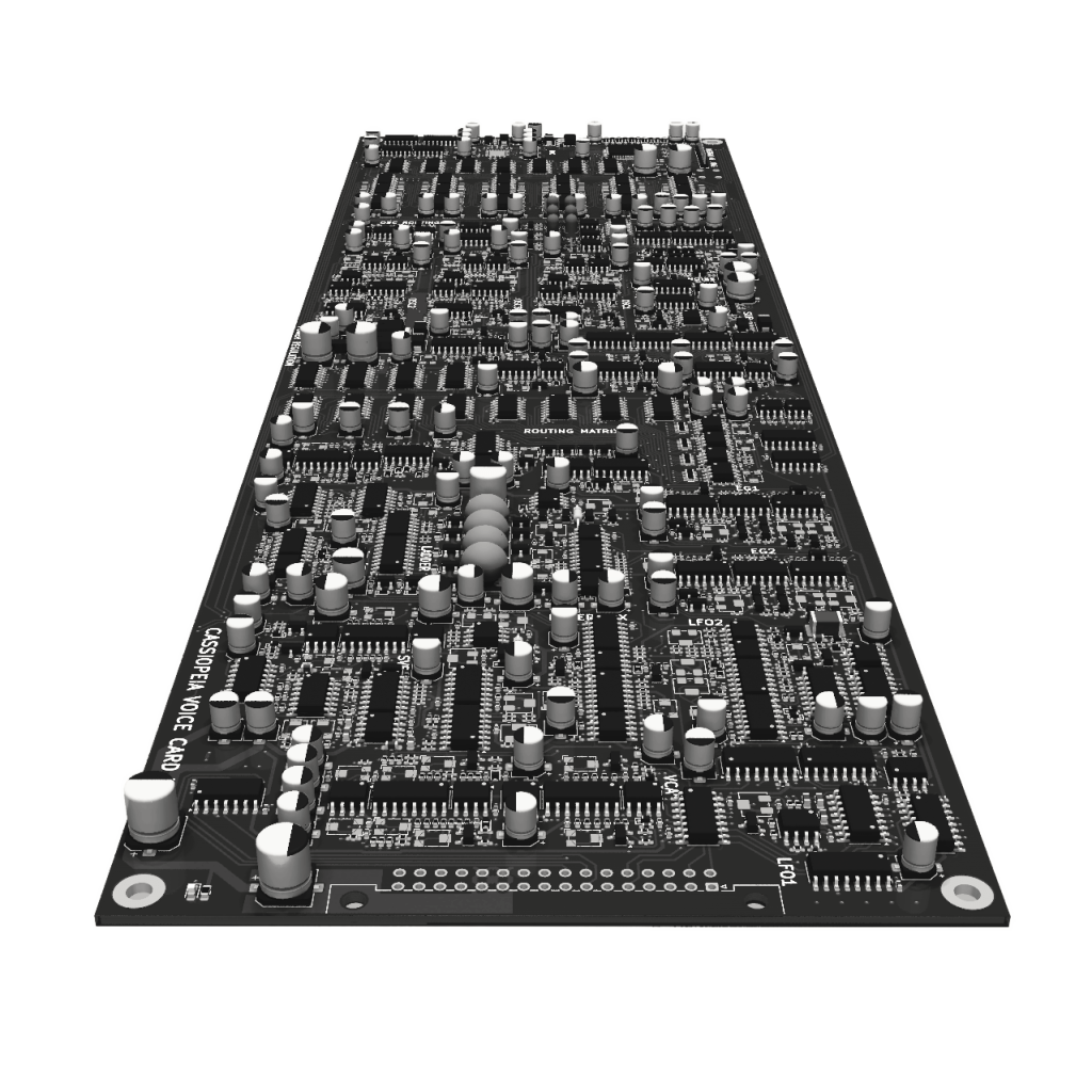
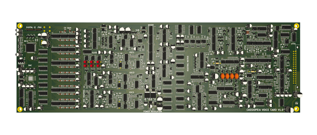
    I have spent the last year prototyping and designing the different building blocks of the analogue circuitry and I am currently finalising the first version of the voice card in KiCad. It’s an absolute beast and I don’t expect it to work, but I hope to learn enough from its failure that version 2 might just work! It’s an extremely complex board, at least by my metric and is a 6 layer SMD PCB. I’ll make a separate post on this voice card design at some point in the future. Although the majority of the analogue electronics is complete, there is still much to do and I expect the synth won’t be playable for another few months to a year at least.

    Most of the schematics are a blend of things I learnt in books or the internet, trial and error from circuit simulation, and new designs from the top of my head. I’m not an electronic engineer so it’s probably inspired in that order. Many circuits in literature are not designed for poly synths, having potentiometers in the audio path of the circuit. If I do borrow something from somewhere else, often I need to modify the circuit to be voltage controlled, and I tweak a lot of aspects anyway to get the sound or features I want. I’m not trying to reinvent the wheel here, but simply to make a working musical instrument that I might be able to perform with.

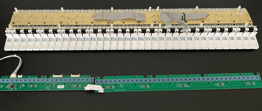
    I’ve also bought a keybed which supports polyphonic aftertouch. You would not believe how hard it is to source a keybed like that unless you are an established company, manufacturers just do not want to sell to individuals or let me know anything about the internal mechanisms! After months of trying to source from a supplier, I gave up and bought a Korg Keystage 61. I didn’t want to get too attached to it so almost immediately I took it apart and scavenged it for the keybed and pressure sensors that implement the poly aftertouch. I still haven’t got round to figuring out how to wire it up to my synth, although the keybed has a suspicious wire coming from it labelled UART which I expect is simply MIDI out. As for the pressure sensors, that’s a whole new adventure…

    Now that’s plenty of waffle, I think that’ll do for a first post. I doubt many will read this and doubt further that they’d be interested in what I have to say, but on the off chance you are invested, feel free to reach out to my email and ask any questions. Also, I desperately need a name for the damn thing, any suggestions welcome!

    Contact

  • Voice Card

    Since receiving the first prototypes of the voice cards nearly two months ago, I’ve been hard at work in my free time trying to get it going. The hardest part of the synth was always going to be the digital to analogue interfacing for the control voltages. I had very little issues getting the shift registers to work, however the DAC presented some issues. Every time I’d solder in a new DAC and boot up the voice card, the current would spike nearly 300 mA above expected and then the DAC seemed to flatline. After another attempt at this, I consulted the data sheet again and noticed that the EPAD on the bottom of the package should be tied to V- and I had falsely assumed it would be GND. No wonder it wasn’t happy. In addition, I forgot the chip select line for the SPI. The latter was fixed with a bodged wire but there wasn’t much I could do to change the GND pad to V- as I couldn’t fit a wire in no matter how much I tried . 

    Another issue I noticed was the oscillators were getting rather hot. I hadn’t noticed this on the through hole prototypes but now it was SMD it was apparent something was unhappy. Turns out, that was the LM319 I was using for the integrator comparator in the sawtooth generator. The LM311 is often historically used for this purpose and it looked as though the LM319 was very similar with tighter timing specs so I used that in place. Unfortunately, the absolute maximum voltages are decreased somewhat compared to the original LM311 and so I was well out of spec. It’s a Christmas miracle that the oscillator worked with no issues other than a bit of heat. I suppose I didn’t notice on the THT version as the package is much bigger than the SOIC and so the heat was dissipated easier. Given this, I decided to go back to the tried and trusted LM311. The slower response time will make little difference in the reset time of the sawtooth as it’s not the bottleneck there. 

    Finally, I had a few tiny 0201 8 resistor arrays that I used for the mixer. JLCPCB didn’t have this in stock when I was ordering the PCB so I thought fine I’ll solder it myself. What. A. Nightmare. I spent probably 2-3 hours just trying to get these four ICs in place without solder bridging, and to make things worse the pinout was incorrect. I decided to do without these and just go with 1% resistors instead so JLCPCB can assemble it for me and I never have to look at that part of the PCB again.

    With these changes in mind, I ordered a new PCB with just the digital electronics and a single oscillator to see if my problems were fixed. After a few failed attempts at soldering the DAC to the PCB (it’s really very small), I successfully managed to communicate to it via SPI. The oscillator was running much cooler as well thanks to the LM311. I tried to implement the multiplexer S+H circuitry to a DAC channel and found to my surprise it worked with suspiciously little issue. The image the left shows the repeating multiplexed output of the DAC on the oscilloscope. This signal is then sampled by each S+H stage to create 8 distinct CVs and fed to the appropriate circuitry. The timing has to be quite tight for this, and I have some more experimentation to do in this regard.

    I did find that during transition from one multiplex output to another, the DAC voltage would change slower than the multiplexer output would switch resulting in periodic spikes in the sample and hold output at the frequency of the multiplex switching. The spikes are small and but I still really don’t like them there. There are two things I can do to mitigate them. The first is to make use of the multiplexer inhibit line to ensure the input of the DAC doesn’t make it to any multiplexer output whilst it’s settling. The second thing I can do is increase the frequency of the multiplex switching. This has the effect of requiring smaller S+H caps and therefore smaller compensation capacitors by DAC outputs allowing the slew rate of the DAC outputs to increase somewhat. I opted to change the S+H caps from a relaxed 100nF to 4n7 so that I can test the multiplexing at a much higher frequency closer to what it will end up at. 

    Now that I’m satisfied with the digital side worked as expected and having the oscillator perform much happier I’ve gathered what information I can from the first voice card prototype and tweak resistor values for the second prototype. Of course, I can only do so much without a working DAC on the original board. A major improvement on this new design is the addition of +/-12V power planes on two new layers. This equates to a £50 increase in PCB price (reduced to £10 per board if I’m ordering 16). I think the price is reasonable to the lower power impedance, better EMI performance, and reduced trace cramming on the signal layers. I’m hoping the planes will also act as big capacitors between each other to help smooth power spikes. The PCB stack up is now:

    1. Analogue signals and components
    2. GND
    3. Digital signals with GND fill
    4. +12V
    5. -12V
    6. Digital signals with GND fill
    7. GND
    8. Analogue signals and test points

    I have also added a few extra features like assignable PW modulation from all mod sources, and a few more routing options for the oscillators and sample and hold source in LFO2.

    I’ve ordered the new board (V2.2) today and await its eager arrival soon. In the meantime I’ve also been designing the front panel, and the PCB to go underneath it.

    Front Panel

    Here she is! I’m currently working with a guy in the UK to bring this to life. The blue is to be matte anodised aluminium, and the light brown to be a polished bronze. I’m thinking the best way to manufacture is to have a 2-3mm thick aluminium base and fit the bronze and anodised aluminium on top like a jigsaw. That way I don’t have to get the bronze at a thickness more than a fraction of a millimetre as anything more is quite expensive. The circle in the middle is to be a 4/5 inch OLED. I’m not a graphic designer so ANY suggestions welcome. I want a regal theme but I’m thinking about adding more spacefaring/seafaring symbols to add detail and to complement its name – Cassiopeia. I initially thought about having motorised knobs like the folks at Melbourne instruments do but after some research it will likely be a good 6 months of R+D for me and I’d rather get the thing built first. Motorised knobs use drone motors and an optical encoder attached to realise absolute position of the knob. This is fine, expect the optical encoder pattern has to be quite high resolution, at least 12 bits, so the pattern must be quite complex and will likely involve some 3D printing to make the enclosure for the optical encoder and associated PCB. So maybe an upgrade for the future and I’ll think about how I can future proof it to include this if I ever want to at a later date.

    The synth will have two keyboards. An upper manual of 61 keys with polyphonic aftertouch, and a lower manual of 88 keys with monophonic aftertouch. The reason for a 88 key lower manual is that the stereo EXT inputs on the synth can be selected to instead be the output of a sampler/ROMpler that will be added internally in the future. Here’s an earlier version of the synth with the keyboards attached – a very early look as to what it might look like. As you can see I haven’t quite decided on a green or blue for the base colour (thoughts welcome!). The other thing you may notice is the knobs are probably quite big in reality (consider it is nearly a metre and a half across according to the 88 key lower manual). The dark brown on the sides will be stained walnut and will be embellished further.

    Power supply

    Finally, a word on PSUs. I originally wanted to go linear and didn’t mind paying for the transformer to do it. However, I have since done some simple maths. The voice card V1.0 draws around 0.6A from the +12 and -12 volt rail when stable. It is fairly consistent here as most synths are. If you multiply by 16 thats already 10 amps per rail, not to mention the front panel, master control board, IO board, and effects. In all I’d expect I’d need to provide 20A to each rail to be safe. For a single transformer, thats at least a 800VA rating, probably higher when you take rectification and regulation drops into account. That’s a big, heavy transformer and hot, inefficient voltage regulation.

    SMPS has improved massively in the last few years, and exhibit much less EMF issues, especially for medical grade supplies. They are far cheaper, and more powerful. The only disadvantage seems to be they can’t handle spikes as well, but this isn’t a power amp, it’s a synth and therefore is quite stable in terms of power draw. I’m thinking of getting two 12V 20A meanwell medical grade supplies and wiring them together properly. I’m not going to try and build one myself unlike if it were a linear supply (I do like the idea of being able to play the synth one day and not have too premature a death!). I’d probably still need some kind of active cooling for the electronics inside, but some small, quiet fans on the rear ought to do.

    The other thing to consider is 0.6A is quite a lot per voice card (considering I need 16 of them). I’ve realised I use rather a lot of NE5532s which have a fairly high quiescent current compared to the TL072. I’ve therefore changed them out for the TL series where possible and tweaked resistor values to aid with power draw. I’m hoping V2.2 can shave nearly 100mA off the draw current from each rail.

    That’s all for now, I’ll probably post an update every other month, or whenever there’s a major breakthrough. For now, have a good Christmas, and a happy new year!

    Contact

  • Voltage Controlled Amplifiers (VCAs) are an essential synth module and the backbone of all poly synths. In a typical monophonic synth you’d only have usually one VCA for the amplitude control of the audio at the output to be modulated by the envelope generator or LFO. But in the world of polyphony, there are dozens more working underneath the surface. It is the primary form in which voltage control of many parameters is realised.

    Let us take a simple passive amplifier as example. The circuit (aside from all the input and output buffers and filtering and protection circuitry that it might have) is essentially a potentiometer with an input terminal and ground terminal. The centre tap is taken as the output and depending on the wiper position, a variable resistive divider is formed which changes the amplitude of the input signal that makes it to the output. This very simple circuit might be a great way to vary, for instance, the amount of an LFO being sent to the pitch input of a voltage controlled oscillator; or the mix of said oscillator with a second noise source. If you want to achieve a similar thing in stereo or two channels you can simply use a two gang potentiometer with wipers that are internally coupled. Then as you move the potentiometer, the wipers change the resistance in roughly the same proportion for each channel. Great! What happens though when you need 3, 4, or even 16 controls that need to be adjusted simultaneously? You can’t have a potentiometer with 16 wipers! Instead the simple passive amplifier must become a voltage controlled amplifier so that a single control voltage can be distributed to 16 separate VCAs which in turn control the amount of the LFO signal reaching the oscillators, or other parameters. This, as you can imagine, is quite a pain. VCAs add cost and complexity to the design and also take up precious PCB space. A voltage controlled amplifier can be thought of as a synth building block for any situation where you need to vary the amplitude of a signal, whether that’s a control voltage, or audio signal. Each voice card of my synth in its current form has no less than 30 VCAs within it, controlling a wide variety of parameters, from the amount of FM oscillator A applies to B, to the mix amount between the two filters.

    So how is a VCA made?

    At the simplest level, a VCA could be made from a BJT transistor. This primitive method can be used but has a few caveats: namely the input signal must be properly biased with a DC voltage to ensure the transistor passes the whole signal without clipping; the output also carries a DC bias which must be eliminated. A single BJT can either source or sink current, but not both from a single device. In order to do so, a more complex configuration is needed, using two or more BJTs to deal with bipolar signals, or the output signal could be AC coupled from the single transistor configuration to remove the offset from the DC bias. This method leads to further complications though if the signal being amplified is not AC coupled itself, like an ADSR envelope for example. In addition to this, the usable control range of a BJT is limited the range of a few tens of millivolts at the base between the transistor being fully closed and fully open. This not only leaves it susceptible to noise but also varies from transistor to transistor resulting in a lack of consistency between VCAs. BJTs are also exponential in their response and are sensitive to temperature and not particularly linear and oh god it’s just a mess. Clearly a more refined approach is needed.

    In the modern day, the simplest decision would be to use a 2164 style chip which includes 4 high performance VCAs in a 16 pin package for £5 a chip (or £1.25) per VCA. I seriously considered using these chips for all my VCAs and it would be a sensible design decision, if not for the very point of me building this synth in the first place – to learn big boy electronics. I wanted to find a medium between buying a chip that does it all for you, and mining the actual silicon from the ground to make my own wafers, that would result in me feeling I had learnt and accomplished something. For this section of the project, I decided that medium would be the Operational Transconductance Amplifier (OTA). I nearly shat myself when I first read the name of that, but it’s not as scary as the name suggests. There are many articles and papers that can explain the inner workings of an OTA better than I can (I’ll link some below), but essentially it behaves similarly to a standard operational amplifier with its high impedance differential voltage inputs, but it also includes an extra bias pin which accepts a control current and outputs a current instead of a voltage in response to the bias. It is, in operation, a voltage controlled current source (takes an input voltage and converts it to an output current via a control current). It acts similarly to an ideal BJT transistor but is self biased and can have a bipolar current output. Standard op amps can be used to convert between voltage and current in the right configuration, meaning all you need to build a VCA is a dual op amp handling current conversion for the bias input and output, and an OTA. The only produced OTA today is the LM13700, a rebrand of the classic CA3080 dual OTA found in many vintage synths. The LM13700 also includes a couple of Darlington buffers on chip for current to voltage conversion. The Darlington buffer does work but usually causes more problems than it solves, as it adds some DC offset, and as such is regularly found disconnected on circuit diagrams. If you look in the right places, an LM13700 can be found for 60p, and a decent dual op amp such as an NE5532 for 50p, meaning price per VCA is around 80p, 2/3rd that of the 2164, albeit with inferior specs and larger PCB footprint. 

    The LM13700 also has linearising diodes, which, when energised, extend the possible input signal amplitude before unusable distortion. Thats the thing about the LM13700, it loves to distort. Typically, with the linearising diodes engaged, a signal shouldn’t exceed 100mVpp for usable THD, and it’s even less with the diodes unterminated. Therefore the input signal, which may often be up to +/-5V in synth world, must be attenuated massively and then reamplified at the output – leading to noise.

    This distortion and noise isn’t necessarily a terrible thing, the nerds might argue the distortion from early OTA and op amp chips in vintage synthesisers are precisely what gives them their “analogue warmth”. Some designers even choose to forgo the linearisation diodes in hopes of achieving a “crunchy” VCA sound. The distortion sound is a relatively pleasing soft clipping effect, but in order for it not to be excessive, the input signal must be turned down further leading to increased noise. Due to this, I tend to employ the diodes, especially for any control voltage VCA use cases where we simply want a voltage to be attenuated or amplified without nonlinear peculiarities. 

    Let’s talk numbers

    I thought I’d break down the resistor values being used in my “standard” VCA configuration. This is a very common arrangement of the OTA that can be found dating back to old electro notes papers, but this article explains it well (https://electricdruid.net/design-a-eurorack-vintage-vca-with-the-lm13700/). I have tweaked the resistors to give good signal to noise ratio, low distortion, easy bias adjustment, and 1V control voltage input change corresponding to a 1V change in output voltage (per polarity). My synth usually uses +/-5V signals for both audio and control voltages, but for this VCA configuration, the control voltage is 0-5V. The LM13700 can struggle with bleed-through of the input signal or even CV to the output if the VCA is not fully closed. To counter this, a small negative voltage can be applied to the control voltage input such that when the CV is at 0V, the negative voltage clamps the bias down. This can be done with a constant voltage source such as from the negative power rail. This is easy to implement, but can result in small CVs dropping downwards, which is particularly apparent on long tails of envelopes. On my synth, as the DAC driving the control voltages can swing negatively, I scale the potentiometer on the front panel or internally so “0” is a very small negative voltage to the VCA CV, and then the pot tracks linearly shortly after the knob is turned up from minimum. This keeps the best of both worlds: no drooping at low CV values, and ensures the VCA is off when it needs to be.

    There are 3 sections to this VCA all feeding into or from the OTA. The input stage is a simple voltage divider comprised of R219 and R221 to take the +/-5V input signal down to around 70mVpp which, when using the linearising diodes with a 1mA current results in around 0.2% distortion. Without the diodes this distortion would be near 5% THD! The maximum allowable current through the diodes bias terminal is 2mA, and the datasheet recommends 1mA. A simple current source can be made with a resistor from the positive rail which is not ideal for many reasons, but will do for this application. In the example schematic, R217 serves this purpose. R217 would have to be 12K to achieve 1mA current, but as this particular VCA is an audio VCA, I wanted some distortion to add some sonic interest. By varying the current to the linearising diodes you can essentially increase or decrease the amount of nonlinearity there is. From experimenting, I found 47K works nicely for my purposes, which is around 250uA. Its important to note that varying the current to the diodes also varies the output current, so this must be taken into account. R222 and RV27 connect the non-inverting input to ground, and by varying RV27, the input DC offset can be adjusted.

    The second section is the control stage feeding pin 16 of the LM13700. It is comprised of a summing op amp which combines the control voltages from various sources (a pot and an envelope generator in the case of this example). The op amp also forms a voltage controlled constant current source together with the PNP transistor. The output of this flows through a 6K8 resistor (R213) which is a protection resistor to ensure the maximum current into the OTA bias pin is capped at just under 2mA, the maximum that the chip is rated for. The diode is for negative current protection. When the DAC outputs a negative CV to the VCA to ensure it’s off, the negative voltage would reverse bias the transistor, shortening its lifespan. The diode provides a return path for excessive negative voltage to prevent this. R206 and R207 allow the gain of the current source to be set. The recommended current is 1mA into the LM13700 for a “fully open” VCA; the current configuration gives around 630uA to be safe, but this could be easily changed by changing the value of R206. The capacitor provides slight CV smoothing and helps with noise.

    The final stage of the VCA consists of a transimpedance current to voltage convertor via an opamp. The current output from the OTA on pin 12 is received by the inverting input of an opamp, to maintain phase with the original incoming signal. R215 sets the gain of the output to match the input when the CV is at maximum. Thereby, if the input voltage is +/-5V, the output voltage will be +/-5V when the CV is 5V, and will change by +/-1V for every volt the CV changes. The only other circuitry is decoupling capacitors for the ICs, and a bulk 1uF decoupling for each rail placed close to the assembly.

    The final stage of the VCA consists of a transimpedance current to voltage convertor via an opamp. The current output from the OTA on pin 12 is received by the inverting input of an opamp, to maintain phase with the original incoming signal. R215 sets the gain of the output to match the input when the CV is at maximum. Thereby, if the input voltage is +/-5V, the output voltage will be +/-5V when the CV is 5V, and will change by +/-1V for every volt the CV changes. The only other circuitry is decoupling capacitors for the ICs, and a bulk 1uF decoupling for each rail placed close to the assembly.

    Physically on the PCB, a dual VCA consisting of one LM13700 and two NE5532s takes up 18x22mm with all the other circuitry attached. I think that ought to do for this post, I’ll attach some further reading and resources that helped me with this topic.

    Further Reading

    LM13700 Datasheet: https://www.ti.com/lit/ds/symlink/lm13700.pdf

    Electricdruid Article: https://electricdruid.net/design-a-eurorack-vintage-vca-with-the-lm13700/

    TI OTA deepdive: https://www.ti.com/lit/an/sboa117a/sboa117a.pdf?ts=1758763923281&ref_url=https%253A%252F%252Fwww.google.com%252F

    Single transistor VCA: https://www.vicphysics.org/documents/teachers/bjtamplifierwells.pdf

    Contact

  • I have realised that the skill of engineering is almost entirely in managing trade offs, which I am still far from mastering. This is especially true in a synthesiser, musical instrument, or any project that combines creativity with a technical aspect as many conflicting aspects must be simultaneously juggled around: quality, cost, artistic style, size, weight, etc etc. Every solution has downsides, and more confusingly sometimes these downsides are secretly good. At the start of this project I was obsessed with keeping noise and distortion low in the circuit as this is what’s all over literature and is objectively the best practice. But actually, noise and distortion is to some extent the character of an electronic instrument and to eliminate it is to suck the soul out of the machine. It’s a rather annoying contradiction that after you design a theoretically perfect oscillator, you listen to it and it sounds dull and boring, but if you tweak some resistors and approach the rails of your op amp, or if you run things a little too hot into the vcas you start generating those lovely harmonics that’s associated with analogue synthesis.

    Lines always have to be drawn though, and the hardest part is figuring out what actually does need to be electrically perfect; where to splash the cash on. For example it is probably audibly pleasing to have a certain amount of distortion in the output of an oscillator, but the control voltage and exponential convertor? That should be perfect for a usable musical instrument. Out of tune oscillators certainly have a place in art pop and ambient soundscapes but at a certain point, you’ll need an instrument that can hit a perfect 5th within a few cents and that circuitry certainly can’t have much noise or distortion. In my poly synth, the vast majority of the cost is directed towards the oscillator tuning: the monolithic transistors for the exponential convertor, the trimmer pots for tracking, and the extra circuitry for temperature compensation all add up quickly when you have 48 true analogue oscillators. 

    DACs

    Another place in a poly synth that shouldn’t be overlooked in terms of quality is the digital to analogue conversion. A poly synth almost always has a form of microcontroller to distribute control voltages, generate envelopes and process MIDI information. There are a few ways to interface this into the analogue circuitry but all will have to involve some form of digital to analogue convertor (DAC) at some point.

    Historically DAC channels were expensive and so ye olde poly synths often had a single DAC channel with some clever sample and hold circuitry after. The DAC would output each control voltage for every parameter one after the other, settling in each CV for a set period (typically sub millisecond). This continuously varying signal would enter an array of demultiplexers which is an analogue switch with a single input and multiple outputs. Each output has a capacitor to ground and an op amp voltage follower subsequently. When a CV is momentarily outputted from the DAC as part of the continuous stream, the demux switches to the corresponding output, charging the capacitor to the DAC output voltage, effectively sampling that voltage. Once the DAC switches to the next CV, the demux switches with it, and the capacitor sees an open input of effectively infinite resistance. The input to the op amp is also high impedance, and as such the capacitor holds its voltage and the op amp mirrors this on its output, driving the analogue circuitry down the line with the sampled voltage. 

    Now in the real world of course, an op amp doesn’t have infinite input impedance and the capacitor also has a parasitic loss to ground. As such, the capacitor voltage slowly droops over time and so the voltage must be continuously updated by the DAC after it cycles through all the CVs. The exact timing of this cycle depends on many factors such as how long the DAC output takes to settle, how many CVs there are to update, how long the capacitor takes to charge, and how fast the capacitor droops but is usually on the order of several hundred to several thousand times per second. Better capacitors and op amps also offer less droop and faster acquisition times of the CV. The best op amps are CMOS input as these have higher input impedance than BJT variants, and the op amp should also have low noise and input offset. The best capacitors for sample and hold circuits should have low leakage (for low droop), and low dielectric absorption (for accuracy). You’ll often find quoted on the internet that the best capacitors have a polystyrene dielectric, but these are really expensive and big and not really made anymore. In practice, modern MLCC C0G capacitors perform well enough for this application and have adequate temperature characteristics. X7R caps can be used if you’re tight on budget, but for the sake of a few quid just get the best! Never use electrolytic for this application.

    In the modern day, DAC channels are cheaper and you can find DAC chips with 8 or more channels for a relatively low cost. High end modern synths such as the Moog One use a dedicated DAC channel for every control voltage, but even with today’s low cost chips that can still add up if you’re not buying in bulk. The advantages, however, are threefold: that you don’t have to worry about timing the demux and DAC cycle, board space is reduced from not needing extra demux/opamp chips, and the output will be more accurate as there’s no opamp offset voltage.

    For my synth, I opted for a meet in the middle approach (all about those tradeoffs!). My synth works around the rough eurorack standard (+/-12V rails, +/-5V CV) so I have an 8 channel DAC which natively outputs +/-5V signals so I don’t have to worry about scaling voltages. Each channel then go to 1:8 demux with a sample and hold circuit on the output of each. This allows for 64 parameters maximum which definitely covers the 48 or so my synth has. The opamps are all TL074s for their CMOS input, adequate specs and low low price. For the pitch CVs, I opted for an OPA4134 for its higher specs as those CVs are the most important. I only use 6 of the 8 channels of the DACs for sample and hold circuits, so I assigned the last two channels to the attack and release for the 3rd envelope generator I squeezed in at the end of the design process. You could argue that two of the pitch CVs should be on the direct output of the DACs if I have the option, but I thought I’d rather have 3 oscillators  with the same CV signal chain. Theoretically if I’ve done my design right, it won’t be a problem anyway!

    In this screenshot from the voice card PCB, you can see the DAC chip (middle left), the column of shift registers to the right to control the demux switching, and the sample and hold demux/opamps on the right with capacitors above/below. Not all traces are shown for demo purposes (on a 6 layer board it gets messy fast)

    Bits and bollocks

    There’s some debate over the amount of bits a DAC for CVs should have. Some people are caught up in the new sigma delta DACs that are apparently magically 24 or even 32 bits for very cheap but as Matthew from North Coast Synthesis explains in this article https://northcoastsynthesis.com/news/dacs-and-bit-count/, that’s kind of bollocks and doesn’t even matter. In reality, for CVs, 8-10 bits is enough for most parameters (attack, release, cutoff, etc), and 12 bits is enough for pitch. The DAC I chose (the LTC2686 for you nerds out there) is 16 bit and so is more than enough for any applications. If the output is +/-5V, and each volt represents an octave with my oscillators tuned to 1V/oct, then the resolution of a 16 bit DAC equates to around 0.18 cents of accuracy (65536 DAC for 10 volt range, 83.33mV per note = 546.13 DAC levels per note). Even with the opamp input offset, noise, and parasitics of the capacitor, I can safely say that the DAC won’t be the limiting factor in pitch precision compared to the temperature instability and tuning nightmares of the exponential convertor. But that’s for another day….

    Further reading

    https://northcoastsynthesis.com/news/dacs-and-bit-count/

    https://www.analog.com/media/en/training-seminars/design-handbooks/system-applications-guide/Section4.pdf

    Contact