Voltage Controlled Amplifiers (VCAs) are an essential synth module and the backbone of all poly synths. In a typical monophonic synth you’d only have usually one VCA for the amplitude control of the audio at the output to be modulated by the envelope generator or LFO. But in the world of polyphony, there are dozens more working underneath the surface. It is the primary form in which voltage control of many parameters is realised.
Let us take a simple passive amplifier as example. The circuit (aside from all the input and output buffers and filtering and protection circuitry that it might have) is essentially a potentiometer with an input terminal and ground terminal. The centre tap is taken as the output and depending on the wiper position, a variable resistive divider is formed which changes the amplitude of the input signal that makes it to the output. This very simple circuit might be a great way to vary, for instance, the amount of an LFO being sent to the pitch input of a voltage controlled oscillator; or the mix of said oscillator with a second noise source. If you want to achieve a similar thing in stereo or two channels you can simply use a two gang potentiometer with wipers that are internally coupled. Then as you move the potentiometer, the wipers change the resistance in roughly the same proportion for each channel. Great! What happens though when you need 3, 4, or even 16 controls that need to be adjusted simultaneously? You can’t have a potentiometer with 16 wipers! Instead the simple passive amplifier must become a voltage controlled amplifier so that a single control voltage can be distributed to 16 separate VCAs which in turn control the amount of the LFO signal reaching the oscillators, or other parameters. This, as you can imagine, is quite a pain. VCAs add cost and complexity to the design and also take up precious PCB space. A voltage controlled amplifier can be thought of as a synth building block for any situation where you need to vary the amplitude of a signal, whether that’s a control voltage, or audio signal. Each voice card of my synth in its current form has no less than 30 VCAs within it, controlling a wide variety of parameters, from the amount of FM oscillator A applies to B, to the mix amount between the two filters.
So how is a VCA made?
At the simplest level, a VCA could be made from a BJT transistor. This primitive method can be used but has a few caveats: namely the input signal must be properly biased with a DC voltage to ensure the transistor passes the whole signal without clipping; the output also carries a DC bias which must be eliminated. A single BJT can either source or sink current, but not both from a single device. In order to do so, a more complex configuration is needed, using two or more BJTs to deal with bipolar signals, or the output signal could be AC coupled from the single transistor configuration to remove the offset from the DC bias. This method leads to further complications though if the signal being amplified is not AC coupled itself, like an ADSR envelope for example. In addition to this, the usable control range of a BJT is limited the range of a few tens of millivolts at the base between the transistor being fully closed and fully open. This not only leaves it susceptible to noise but also varies from transistor to transistor resulting in a lack of consistency between VCAs. BJTs are also exponential in their response and are sensitive to temperature and not particularly linear and oh god it’s just a mess. Clearly a more refined approach is needed.
In the modern day, the simplest decision would be to use a 2164 style chip which includes 4 high performance VCAs in a 16 pin package for £5 a chip (or £1.25) per VCA. I seriously considered using these chips for all my VCAs and it would be a sensible design decision, if not for the very point of me building this synth in the first place – to learn big boy electronics. I wanted to find a medium between buying a chip that does it all for you, and mining the actual silicon from the ground to make my own wafers, that would result in me feeling I had learnt and accomplished something. For this section of the project, I decided that medium would be the Operational Transconductance Amplifier (OTA). I nearly shat myself when I first read the name of that, but it’s not as scary as the name suggests. There are many articles and papers that can explain the inner workings of an OTA better than I can (I’ll link some below), but essentially it behaves similarly to a standard operational amplifier with its high impedance differential voltage inputs, but it also includes an extra bias pin which accepts a control current and outputs a current instead of a voltage in response to the bias. It is, in operation, a voltage controlled current source (takes an input voltage and converts it to an output current via a control current). It acts similarly to an ideal BJT transistor but is self biased and can have a bipolar current output. Standard op amps can be used to convert between voltage and current in the right configuration, meaning all you need to build a VCA is a dual op amp handling current conversion for the bias input and output, and an OTA. The only produced OTA today is the LM13700, a rebrand of the classic CA3080 dual OTA found in many vintage synths. The LM13700 also includes a couple of Darlington buffers on chip for current to voltage conversion. The Darlington buffer does work but usually causes more problems than it solves, as it adds some DC offset, and as such is regularly found disconnected on circuit diagrams. If you look in the right places, an LM13700 can be found for 60p, and a decent dual op amp such as an NE5532 for 50p, meaning price per VCA is around 80p, 2/3rd that of the 2164, albeit with inferior specs and larger PCB footprint.
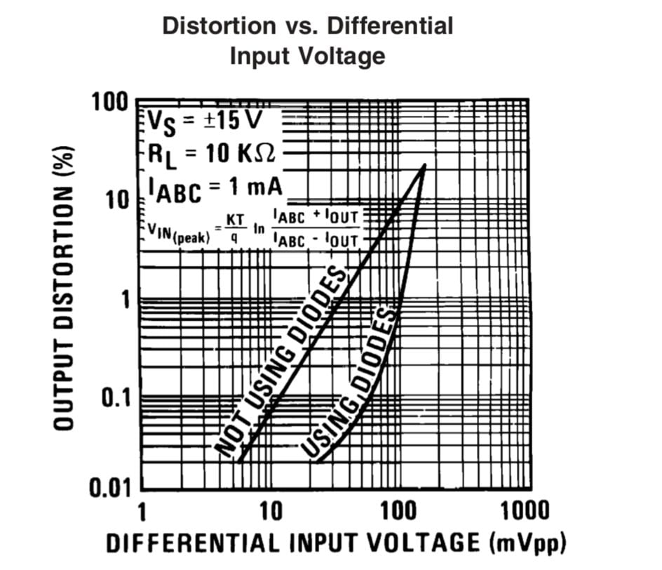
The LM13700 also has linearising diodes, which, when energised, extend the possible input signal amplitude before unusable distortion. Thats the thing about the LM13700, it loves to distort. Typically, with the linearising diodes engaged, a signal shouldn’t exceed 100mVpp for usable THD, and it’s even less with the diodes unterminated. Therefore the input signal, which may often be up to +/-5V in synth world, must be attenuated massively and then reamplified at the output – leading to noise.
This distortion and noise isn’t necessarily a terrible thing, the nerds might argue the distortion from early OTA and op amp chips in vintage synthesisers are precisely what gives them their “analogue warmth”. Some designers even choose to forgo the linearisation diodes in hopes of achieving a “crunchy” VCA sound. The distortion sound is a relatively pleasing soft clipping effect, but in order for it not to be excessive, the input signal must be turned down further leading to increased noise. Due to this, I tend to employ the diodes, especially for any control voltage VCA use cases where we simply want a voltage to be attenuated or amplified without nonlinear peculiarities.
Let’s talk numbers
I thought I’d break down the resistor values being used in my “standard” VCA configuration. This is a very common arrangement of the OTA that can be found dating back to old electro notes papers, but this article explains it well (https://electricdruid.net/design-a-eurorack-vintage-vca-with-the-lm13700/). I have tweaked the resistors to give good signal to noise ratio, low distortion, easy bias adjustment, and 1V control voltage input change corresponding to a 1V change in output voltage (per polarity). My synth usually uses +/-5V signals for both audio and control voltages, but for this VCA configuration, the control voltage is 0-5V. The LM13700 can struggle with bleed-through of the input signal or even CV to the output if the VCA is not fully closed. To counter this, a small negative voltage can be applied to the control voltage input such that when the CV is at 0V, the negative voltage clamps the bias down. This can be done with a constant voltage source such as from the negative power rail. This is easy to implement, but can result in small CVs dropping downwards, which is particularly apparent on long tails of envelopes. On my synth, as the DAC driving the control voltages can swing negatively, I scale the potentiometer on the front panel or internally so “0” is a very small negative voltage to the VCA CV, and then the pot tracks linearly shortly after the knob is turned up from minimum. This keeps the best of both worlds: no drooping at low CV values, and ensures the VCA is off when it needs to be.
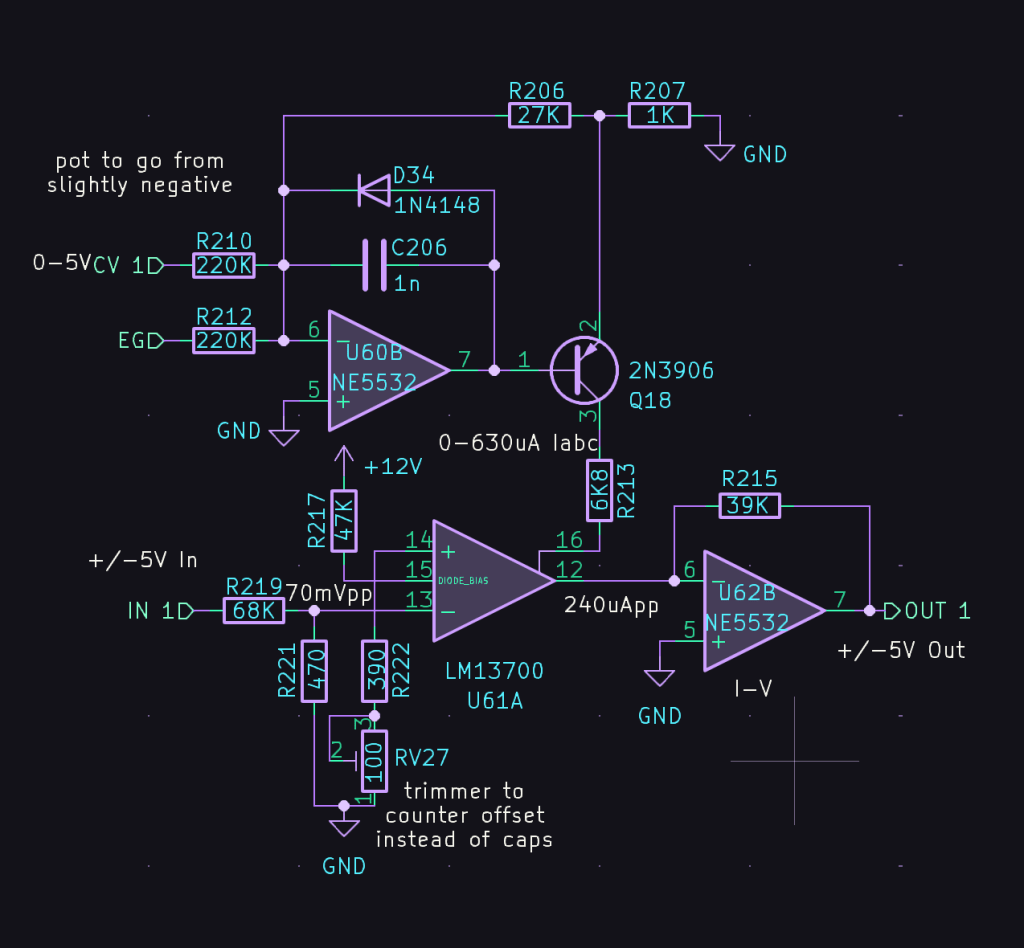
There are 3 sections to this VCA all feeding into or from the OTA. The input stage is a simple voltage divider comprised of R219 and R221 to take the +/-5V input signal down to around 70mVpp which, when using the linearising diodes with a 1mA current results in around 0.2% distortion. Without the diodes this distortion would be near 5% THD! The maximum allowable current through the diodes bias terminal is 2mA, and the datasheet recommends 1mA. A simple current source can be made with a resistor from the positive rail which is not ideal for many reasons, but will do for this application. In the example schematic, R217 serves this purpose. R217 would have to be 12K to achieve 1mA current, but as this particular VCA is an audio VCA, I wanted some distortion to add some sonic interest. By varying the current to the linearising diodes you can essentially increase or decrease the amount of nonlinearity there is. From experimenting, I found 47K works nicely for my purposes, which is around 250uA. Its important to note that varying the current to the diodes also varies the output current, so this must be taken into account. R222 and RV27 connect the non-inverting input to ground, and by varying RV27, the input DC offset can be adjusted.
The second section is the control stage feeding pin 16 of the LM13700. It is comprised of a summing op amp which combines the control voltages from various sources (a pot and an envelope generator in the case of this example). The op amp also forms a voltage controlled constant current source together with the PNP transistor. The output of this flows through a 6K8 resistor (R213) which is a protection resistor to ensure the maximum current into the OTA bias pin is capped at just under 2mA, the maximum that the chip is rated for. The diode is for negative current protection. When the DAC outputs a negative CV to the VCA to ensure it’s off, the negative voltage would reverse bias the transistor, shortening its lifespan. The diode provides a return path for excessive negative voltage to prevent this. R206 and R207 allow the gain of the current source to be set. The recommended current is 1mA into the LM13700 for a “fully open” VCA; the current configuration gives around 630uA to be safe, but this could be easily changed by changing the value of R206. The capacitor provides slight CV smoothing and helps with noise.
The final stage of the VCA consists of a transimpedance current to voltage convertor via an opamp. The current output from the OTA on pin 12 is received by the inverting input of an opamp, to maintain phase with the original incoming signal. R215 sets the gain of the output to match the input when the CV is at maximum. Thereby, if the input voltage is +/-5V, the output voltage will be +/-5V when the CV is 5V, and will change by +/-1V for every volt the CV changes. The only other circuitry is decoupling capacitors for the ICs, and a bulk 1uF decoupling for each rail placed close to the assembly.
The final stage of the VCA consists of a transimpedance current to voltage convertor via an opamp. The current output from the OTA on pin 12 is received by the inverting input of an opamp, to maintain phase with the original incoming signal. R215 sets the gain of the output to match the input when the CV is at maximum. Thereby, if the input voltage is +/-5V, the output voltage will be +/-5V when the CV is 5V, and will change by +/-1V for every volt the CV changes. The only other circuitry is decoupling capacitors for the ICs, and a bulk 1uF decoupling for each rail placed close to the assembly.
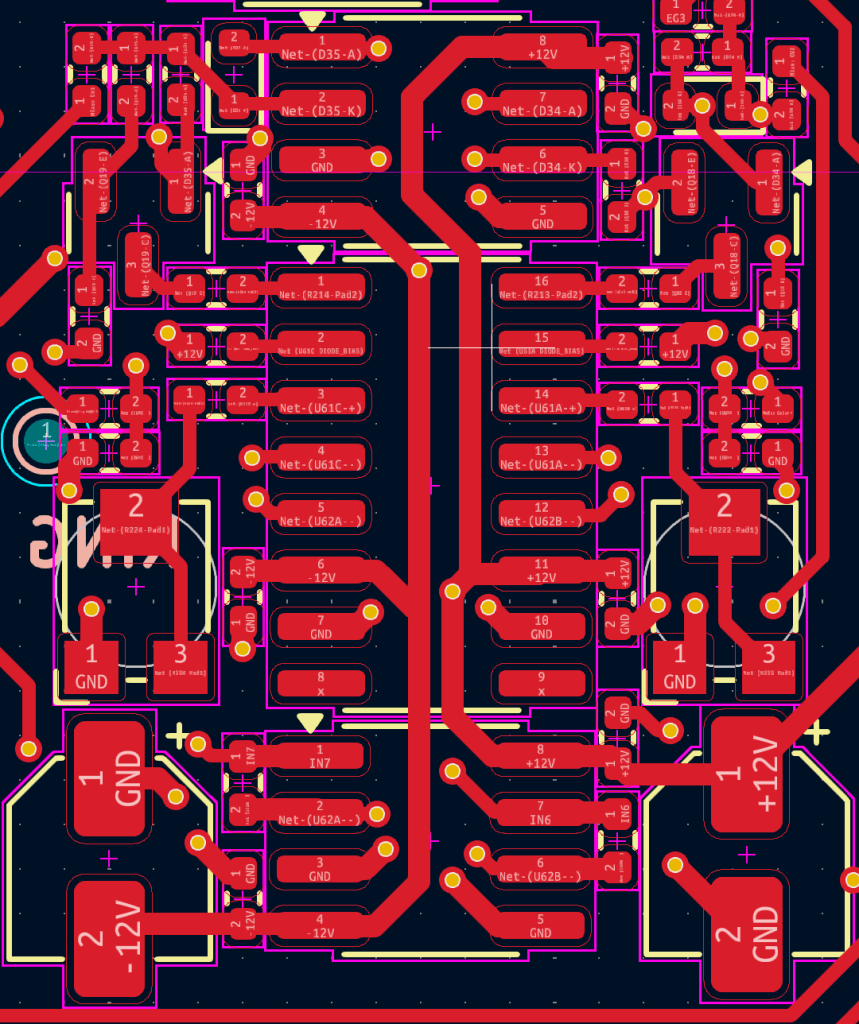
Physically on the PCB, a dual VCA consisting of one LM13700 and two NE5532s takes up 18x22mm with all the other circuitry attached. I think that ought to do for this post, I’ll attach some further reading and resources that helped me with this topic.
Further Reading
LM13700 Datasheet: https://www.ti.com/lit/ds/symlink/lm13700.pdf
Electricdruid Article: https://electricdruid.net/design-a-eurorack-vintage-vca-with-the-lm13700/
TI OTA deepdive: https://www.ti.com/lit/an/sboa117a/sboa117a.pdf?ts=1758763923281&ref_url=https%253A%252F%252Fwww.google.com%252F
Single transistor VCA: https://www.vicphysics.org/documents/teachers/bjtamplifierwells.pdf
