Voice Card
Since receiving the first prototypes of the voice cards nearly two months ago, I’ve been hard at work in my free time trying to get it going. The hardest part of the synth was always going to be the digital to analogue interfacing for the control voltages. I had very little issues getting the shift registers to work, however the DAC presented some issues. Every time I’d solder in a new DAC and boot up the voice card, the current would spike nearly 300 mA above expected and then the DAC seemed to flatline. After another attempt at this, I consulted the data sheet again and noticed that the EPAD on the bottom of the package should be tied to V- and I had falsely assumed it would be GND. No wonder it wasn’t happy. In addition, I forgot the chip select line for the SPI. The latter was fixed with a bodged wire but there wasn’t much I could do to change the GND pad to V- as I couldn’t fit a wire in no matter how much I tried .
Another issue I noticed was the oscillators were getting rather hot. I hadn’t noticed this on the through hole prototypes but now it was SMD it was apparent something was unhappy. Turns out, that was the LM319 I was using for the integrator comparator in the sawtooth generator. The LM311 is often historically used for this purpose and it looked as though the LM319 was very similar with tighter timing specs so I used that in place. Unfortunately, the absolute maximum voltages are decreased somewhat compared to the original LM311 and so I was well out of spec. It’s a Christmas miracle that the oscillator worked with no issues other than a bit of heat. I suppose I didn’t notice on the THT version as the package is much bigger than the SOIC and so the heat was dissipated easier. Given this, I decided to go back to the tried and trusted LM311. The slower response time will make little difference in the reset time of the sawtooth as it’s not the bottleneck there.
Finally, I had a few tiny 0201 8 resistor arrays that I used for the mixer. JLCPCB didn’t have this in stock when I was ordering the PCB so I thought fine I’ll solder it myself. What. A. Nightmare. I spent probably 2-3 hours just trying to get these four ICs in place without solder bridging, and to make things worse the pinout was incorrect. I decided to do without these and just go with 1% resistors instead so JLCPCB can assemble it for me and I never have to look at that part of the PCB again.
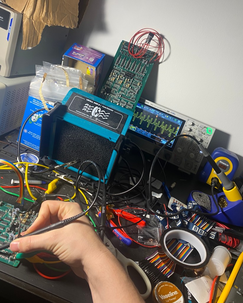
With these changes in mind, I ordered a new PCB with just the digital electronics and a single oscillator to see if my problems were fixed. After a few failed attempts at soldering the DAC to the PCB (it’s really very small), I successfully managed to communicate to it via SPI. The oscillator was running much cooler as well thanks to the LM311. I tried to implement the multiplexer S+H circuitry to a DAC channel and found to my surprise it worked with suspiciously little issue. The image the left shows the repeating multiplexed output of the DAC on the oscilloscope. This signal is then sampled by each S+H stage to create 8 distinct CVs and fed to the appropriate circuitry. The timing has to be quite tight for this, and I have some more experimentation to do in this regard.
I did find that during transition from one multiplex output to another, the DAC voltage would change slower than the multiplexer output would switch resulting in periodic spikes in the sample and hold output at the frequency of the multiplex switching. The spikes are small and but I still really don’t like them there. There are two things I can do to mitigate them. The first is to make use of the multiplexer inhibit line to ensure the input of the DAC doesn’t make it to any multiplexer output whilst it’s settling. The second thing I can do is increase the frequency of the multiplex switching. This has the effect of requiring smaller S+H caps and therefore smaller compensation capacitors by DAC outputs allowing the slew rate of the DAC outputs to increase somewhat. I opted to change the S+H caps from a relaxed 100nF to 4n7 so that I can test the multiplexing at a much higher frequency closer to what it will end up at.
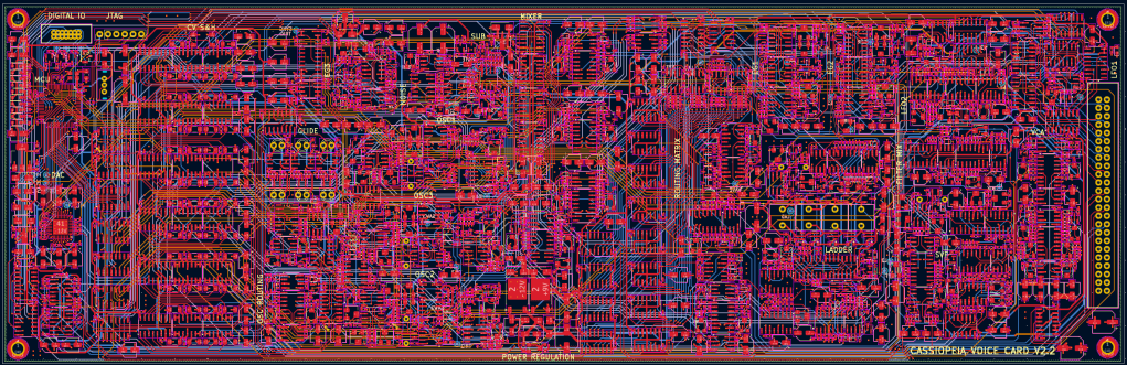
Now that I’m satisfied with the digital side worked as expected and having the oscillator perform much happier I’ve gathered what information I can from the first voice card prototype and tweak resistor values for the second prototype. Of course, I can only do so much without a working DAC on the original board. A major improvement on this new design is the addition of +/-12V power planes on two new layers. This equates to a £50 increase in PCB price (reduced to £10 per board if I’m ordering 16). I think the price is reasonable to the lower power impedance, better EMI performance, and reduced trace cramming on the signal layers. I’m hoping the planes will also act as big capacitors between each other to help smooth power spikes. The PCB stack up is now:
- Analogue signals and components
- GND
- Digital signals with GND fill
- +12V
- -12V
- Digital signals with GND fill
- GND
- Analogue signals and test points
I have also added a few extra features like assignable PW modulation from all mod sources, and a few more routing options for the oscillators and sample and hold source in LFO2.
I’ve ordered the new board (V2.2) today and await its eager arrival soon. In the meantime I’ve also been designing the front panel, and the PCB to go underneath it.
Front Panel
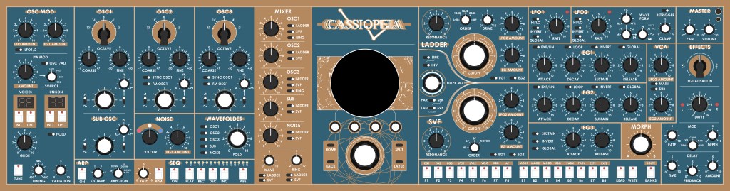
Here she is! I’m currently working with a guy in the UK to bring this to life. The blue is to be matte anodised aluminium, and the light brown to be a polished bronze. I’m thinking the best way to manufacture is to have a 2-3mm thick aluminium base and fit the bronze and anodised aluminium on top like a jigsaw. That way I don’t have to get the bronze at a thickness more than a fraction of a millimetre as anything more is quite expensive. The circle in the middle is to be a 4/5 inch OLED. I’m not a graphic designer so ANY suggestions welcome. I want a regal theme but I’m thinking about adding more spacefaring/seafaring symbols to add detail and to complement its name – Cassiopeia. I initially thought about having motorised knobs like the folks at Melbourne instruments do but after some research it will likely be a good 6 months of R+D for me and I’d rather get the thing built first. Motorised knobs use drone motors and an optical encoder attached to realise absolute position of the knob. This is fine, expect the optical encoder pattern has to be quite high resolution, at least 12 bits, so the pattern must be quite complex and will likely involve some 3D printing to make the enclosure for the optical encoder and associated PCB. So maybe an upgrade for the future and I’ll think about how I can future proof it to include this if I ever want to at a later date.
The synth will have two keyboards. An upper manual of 61 keys with polyphonic aftertouch, and a lower manual of 88 keys with monophonic aftertouch. The reason for a 88 key lower manual is that the stereo EXT inputs on the synth can be selected to instead be the output of a sampler/ROMpler that will be added internally in the future. Here’s an earlier version of the synth with the keyboards attached – a very early look as to what it might look like. As you can see I haven’t quite decided on a green or blue for the base colour (thoughts welcome!). The other thing you may notice is the knobs are probably quite big in reality (consider it is nearly a metre and a half across according to the 88 key lower manual). The dark brown on the sides will be stained walnut and will be embellished further.

Power supply
Finally, a word on PSUs. I originally wanted to go linear and didn’t mind paying for the transformer to do it. However, I have since done some simple maths. The voice card V1.0 draws around 0.6A from the +12 and -12 volt rail when stable. It is fairly consistent here as most synths are. If you multiply by 16 thats already 10 amps per rail, not to mention the front panel, master control board, IO board, and effects. In all I’d expect I’d need to provide 20A to each rail to be safe. For a single transformer, thats at least a 800VA rating, probably higher when you take rectification and regulation drops into account. That’s a big, heavy transformer and hot, inefficient voltage regulation.
SMPS has improved massively in the last few years, and exhibit much less EMF issues, especially for medical grade supplies. They are far cheaper, and more powerful. The only disadvantage seems to be they can’t handle spikes as well, but this isn’t a power amp, it’s a synth and therefore is quite stable in terms of power draw. I’m thinking of getting two 12V 20A meanwell medical grade supplies and wiring them together properly. I’m not going to try and build one myself unlike if it were a linear supply (I do like the idea of being able to play the synth one day and not have too premature a death!). I’d probably still need some kind of active cooling for the electronics inside, but some small, quiet fans on the rear ought to do.
The other thing to consider is 0.6A is quite a lot per voice card (considering I need 16 of them). I’ve realised I use rather a lot of NE5532s which have a fairly high quiescent current compared to the TL072. I’ve therefore changed them out for the TL series where possible and tweaked resistor values to aid with power draw. I’m hoping V2.2 can shave nearly 100mA off the draw current from each rail.
That’s all for now, I’ll probably post an update every other month, or whenever there’s a major breakthrough. For now, have a good Christmas, and a happy new year!
